Vacant Labs and Unfilled Roles: The Atomic-Scale Engineering Talent Crisis Threatening America's Nanotech Ambitions
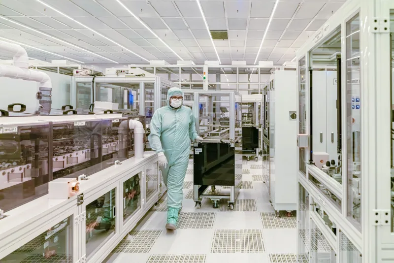
Walk through any cleanroom facility at a semiconductor startup in San Jose, a nanomaterials firm outside Boston, or a defense contractor in Albuquerque, and a recurring frustration surfaces almost immediately: the benches are there, the instruments are calibrated, and the funding has arrived — but the engineers capable of running a meaningful experiment at the sub-100-nanometer scale are nowhere to be found.
This is not a perception problem. Survey data collected by the National Nanotechnology Initiative and corroborated by independent industry polling consistently show that employers in nanoscale fabrication, characterization, and quality assurance report average vacancy periods exceeding five to seven months for mid-level technical roles. In a field where process windows are measured in angstroms and contamination events can invalidate weeks of work, that staffing gap translates directly into delayed product timelines, inflated labor costs, and, in some cases, forfeited federal contracts.
What Employers Are Actually Looking For
The first step toward solving any talent problem is defining it precisely. When hiring managers at nanotechnology firms describe their ideal candidate, they rarely invoke the abstract language of academic curricula. Instead, they cite a remarkably specific constellation of competencies.
Proficiency with characterization instrumentation tops nearly every list. Scanning electron microscopy, transmission electron microscopy, atomic force microscopy, and X-ray photoelectron spectroscopy are no longer exotic tools reserved for flagship research universities — they are production-floor necessities. Yet many engineering graduates arrive having observed these instruments during a single lab demonstration rather than having operated them independently through a full experimental cycle.
Beyond instrumentation, employers emphasize process discipline. Nanoscale fabrication is unforgiving: a photolithography step performed at the wrong humidity, a deposition run with a subtly contaminated precursor, or a quality-control measurement taken with an improperly calibrated tip can cascade into failures that are nearly impossible to diagnose after the fact. The engineers who thrive in these environments possess what several hiring managers describe as "atomic intuition" — a trained sense for how materials behave at scales where quantum effects and surface chemistry dominate over bulk properties.
Data interpretation and statistical process control round out the core skill set. As nanofabrication moves from research prototypes toward scalable production, the ability to distinguish meaningful process drift from measurement noise, and to communicate that distinction clearly to cross-functional teams, has become indispensable.
Where the Academic Pipeline Breaks Down
The United States produces roughly 200,000 engineering bachelor's degrees annually. The overwhelming majority of those graduates concentrate in software, electrical, and mechanical disciplines — fields with well-established industry pipelines, abundant internship opportunities, and clear compensation trajectories. Nanoscience and nanoscale engineering programs, by contrast, remain comparatively rare and are often embedded within materials science or physics departments, where they compete for resources and visibility.
The problem is not simply enrollment numbers. It is curricular architecture. Traditional materials science programs were designed around bulk properties — tensile strength, thermal conductivity, corrosion resistance — because those were the properties that mattered to the industries funding university research throughout the twentieth century. Integrating nanoscale fabrication into that framework requires not only new course content but new laboratory infrastructure, which carries a price tag that many institutions struggle to justify when student demand appears modest.
There is also a feedback loop problem. Students choose majors partly based on perceived employment prospects, and nanotech roles — while genuinely plentiful and well-compensated — are less visible to undergraduates than positions at software companies that recruit aggressively on campus. Without exposure, interest does not develop; without interest, enrollment stays flat; without enrollment, departments cannot make the case for capital investment in advanced characterization suites.
Universities Moving the Needle
A handful of institutions are demonstrating that the curricular inertia can be overcome. The University of California, Berkeley has integrated fabrication modules directly into its undergraduate materials science sequence, giving students scheduled access to the Marvell Nanofabrication Laboratory rather than treating cleanroom time as a graduate-level privilege. MIT's Research Laboratory of Electronics has similarly restructured portions of its nanoscience coursework around project-based learning, where teams move a device concept from design through characterization over the course of a semester.
Georgia Tech's Institute for Electronics and Nanotechnology has pursued a different model, building structured industry partnerships that place undergraduates in supervised fabrication roles during summer terms. Students return to campus with practical experience that is immediately legible to employers — and with professional networks that accelerate hiring upon graduation.
Purdue University deserves particular mention for its investment in quantum and nanoscale engineering tracks within its electrical and computer engineering college, supported in part by funding aligned with the CHIPS and Science Act. That federal legislation, signed in 2022, allocated significant resources toward workforce development in advanced manufacturing, and forward-looking universities have moved quickly to capture those dollars.
The Bootcamp and Certification Frontier
For professionals already holding engineering degrees who need to pivot into nanoscale roles, a new category of accelerated training programs is beginning to emerge. These are not the coding bootcamps of the software world — they require genuine scientific foundations — but they share the philosophy of intensive, application-focused instruction designed to produce job-ready competencies in months rather than years.
The American Vacuum Society and the Microscopy Society of America both offer structured professional development pathways, though critics note these tend to target specialists who are already working in adjacent fields. More ambitious is the model being piloted by several national laboratories, including Argonne and Sandia, which have begun offering structured fellowship tracks for engineers transitioning from aerospace, semiconductor, or biomedical backgrounds into nanoscale fabrication roles. These programs combine instrument training with mentored project work and, critically, with exposure to the quality-management frameworks that production environments demand.
Private-sector initiatives are also emerging. A small number of startups focused on nanofabrication tooling have begun offering paid residency programs — essentially apprenticeships — structured around their own equipment platforms. While critics point out that such programs risk producing engineers who are fluent in one vendor's workflow but limited outside it, proponents argue that any practical experience is preferable to none.
A Structural Problem Requiring Structural Solutions
The talent gap in atomic-scale engineering will not be resolved by any single intervention. It requires simultaneous action across the academic, federal, and private sectors — updated curricula, sustained capital investment in university cleanrooms, visible career pathways for undergraduates, and industry willingness to co-invest in workforce development rather than simply lamenting its absence.
What is clear is that the stakes extend well beyond the balance sheets of individual companies. The United States has staked considerable geopolitical and economic capital on maintaining leadership in advanced nanomanufacturing — from semiconductor fabrication to nanomedicine to next-generation defense materials. That leadership cannot be sustained by instruments alone. It requires the human expertise to operate them, interpret what they reveal, and translate those insights into reproducible, scalable processes.
The cleanroom benches are ready. The question is whether the engineers to fill them will arrive in time.