After Silicon: How Nanoscale Engineering Is Charting the Next Decade of American Computing
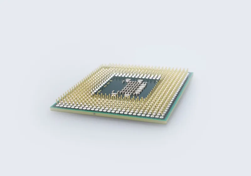
For most of the computing era, progress followed a dependable rhythm. Every eighteen to twenty-four months, engineers managed to pack roughly twice as many transistors onto a silicon chip of the same area, delivering predictable gains in processing speed and energy efficiency. Gordon Moore's 1965 observation about this doubling cadence became an industry organizing principle—a roadmap that chipmakers, software developers, and hardware architects all planned around.
That rhythm has broken down. Physical constraints at the atomic scale—quantum tunneling, heat dissipation, and the fundamental limits of lithographic patterning—have made it progressively harder and more expensive to continue shrinking silicon transistors. The industry has not stopped advancing, but the nature of advancement has changed. The gains that once came from simply making transistors smaller now require fundamentally different architectural and materials strategies. Many of those strategies are built on nanoscale engineering breakthroughs that represent some of the most consequential materials science work of the current decade.
Why Silicon Is Running Out of Room
Modern high-performance silicon transistors operate at gate lengths approaching two nanometers—a dimension so small that the channel region contains only a handful of silicon atoms. At that scale, quantum mechanical effects that engineers once treated as negligible become dominant. Electrons tunnel through insulating barriers that should block them. Thermal energy at room temperature becomes comparable to the energy differences that define transistor switching states. Leakage currents that waste power and generate heat become increasingly difficult to suppress.
Manufacturing complexity compounds the physical challenges. Producing chips at the two-nanometer node requires extreme ultraviolet lithography systems that cost upward of $350 million per unit, operate in near-vacuum environments, and demand tolerances measured in fractions of a nanometer across wafers spanning three hundred millimeters. The capital requirements have narrowed the field of companies capable of leading-edge fabrication to a small number of global players, with significant implications for American industrial and national security interests.
The semiconductor industry's response has not been to concede defeat but to pursue multiple parallel strategies for sustaining performance gains through means other than simple transistor miniaturization. Several of those strategies are now transitioning from research laboratories to commercial production.
Three-Dimensional Architectures: Building Upward Instead of Inward
The most immediately impactful departure from conventional planar scaling involves stacking functional layers vertically rather than continuing to shrink features horizontally. Three-dimensional chip architectures—encompassing both three-dimensional NAND flash memory, which has been in commercial production for nearly a decade, and more recently three-dimensional logic and packaging approaches—allow engineers to increase transistor density and interconnect bandwidth without requiring further reduction in individual feature dimensions.
Intel's Foveros technology, TSMC's System-on-Integrated-Chips packaging, and AMD's chiplet-based processor designs all represent commercial implementations of this principle. By disaggregating a monolithic chip into smaller functional dies—chiplets—and connecting them through dense arrays of microscale copper pillars or hybrid bonding interfaces, manufacturers can combine components fabricated at different process nodes into a single package that performs as an integrated whole.
The nanoscale engineering challenge in three-dimensional integration lies primarily in the interconnects. Traditional wire bonding and solder bump connections between chip layers introduce latency and power consumption that undermine the performance benefits of stacking. Hybrid bonding—a technique in which copper-to-copper connections are formed at pitches below ten micrometers through a combination of surface polishing, chemical-mechanical planarization, and thermal annealing—enables interconnect densities orders of magnitude higher than conventional packaging approaches. Achieving reliable hybrid bonds requires surface roughness control at the sub-nanometer level across the full wafer area, a materials engineering challenge of considerable sophistication.
Photonic Computing: Moving Data at the Speed of Light
A separate but complementary approach to the post-silicon computing challenge involves replacing electrical signals with photons for data transmission, both within and between chips. Photonic interconnects—waveguides, modulators, and photodetectors fabricated from silicon photonics or emerging materials platforms—can carry data at the speed of light with substantially lower energy consumption per bit than copper electrical interconnects.
The fundamental advantage of photonic data transmission derives from physics: photons do not generate resistive heating losses as they propagate through a waveguide, and they can be multiplexed across multiple wavelengths simultaneously, dramatically increasing bandwidth without proportionally increasing power consumption. For data centers—where interconnect energy accounts for an increasingly large fraction of total power consumption—photonic solutions offer compelling efficiency gains.
Materials science is central to realizing photonic computing at scale. Silicon itself is an inefficient light emitter, which has historically limited the integration of light sources with silicon photonic waveguides. Research programs at MIT, Stanford, and several national laboratories are investigating alternative materials—including germanium-tin alloys, III-V semiconductor heterostructures grown on silicon substrates, and two-dimensional materials such as transition metal dichalcogenides—that can serve as efficient on-chip light sources compatible with existing semiconductor manufacturing infrastructure.
Intel, which has invested in silicon photonics for more than two decades, demonstrated co-packaged optical transceivers for data center switching in 2023. The technology integrates optical engines directly with switch ASICs, reducing the electrical path length for high-bandwidth signals and enabling port densities that purely electrical architectures cannot match.
Carbon Nanotubes and the Alternative Transistor
Perhaps the most structurally radical post-silicon computing technology involves replacing silicon as the transistor channel material entirely. Carbon nanotube field-effect transistors have attracted sustained research interest for more than twenty years, based on theoretical predictions—now substantially confirmed experimentally—that carbon nanotube transistors can achieve higher carrier mobility, lower operating voltage, and greater energy efficiency than equivalent silicon devices.
The practical challenge has been manufacturing. Carbon nanotubes grown by chemical vapor deposition are produced as mixtures of semiconducting and metallic species, with variable chirality that determines their electronic properties. Depositing a uniform layer of semiconducting nanotubes in precise alignment across a wafer, at densities sufficient for dense logic circuits, has proven extraordinarily difficult.
Researchers at MIT reported a significant advance in 2019 with the demonstration of a sixteen-bit carbon nanotube processor fabricated using a technique that selectively removes metallic nanotubes and deposits aligned semiconducting tubes across a wafer. IBM's research division has published work on carbon nanotube transistors with gate lengths below ten nanometers that outperform silicon devices of equivalent dimensions on key energy-delay metrics.
Commercial production of carbon nanotube logic remains years away, but the trajectory of the research is encouraging, and the US national laboratory system—particularly Argonne and Oak Ridge—has continued to invest in characterization and synthesis capabilities that underpin the field.
The Competitiveness Imperative
For the United States, the post-silicon computing transition carries strategic weight that extends well beyond corporate market share. Advanced computing hardware underpins artificial intelligence training, cryptography, signals intelligence, and precision manufacturing—domains where computational performance directly translates to national capability.
The CHIPS and Science Act represents a significant federal commitment to rebuilding domestic semiconductor manufacturing capacity, but the deeper challenge involves sustaining American leadership in the underlying materials science and nanoscale engineering that will define what comes after current-generation silicon. That requires not only fabrication facilities but the research infrastructure, workforce, and institutional knowledge to innovate at the atomic scale.
The engineers and scientists working on three-dimensional integration, photonic interconnects, and carbon nanotube transistors are not simply iterating on an existing paradigm. They are constructing the material foundations of the next computing era—one transistor, one photon, and one nanotube at a time.